

The following are the general steps for PCB etching:
Design the PCB layout and generate the corresponding image file using the board design software.
Lay a thin solder mask on the circuit board to protect the copper layer that does not need to be etched.
Using a photosensitive circuit board (also known as a photosensitive circuit board) or a traditional photosensitive coating, the image is transferred to the circuit board
After the etching is complete, the circuit board is removed from the etching solution and rinsed with water.
Remove solder shield or solder shield to facilitate soldering of electronic components.
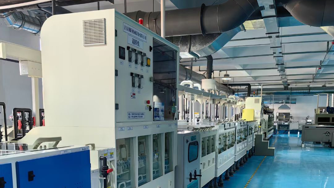
We have professional engineers and QA in all aspects to strictly control the quality.
Post time: Oct-27-2023